Section B: Transistors (BJT)
Q5. Define BJT (Bipolar Junction Transistor) with Symbol.3 Marks
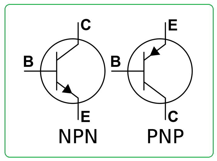
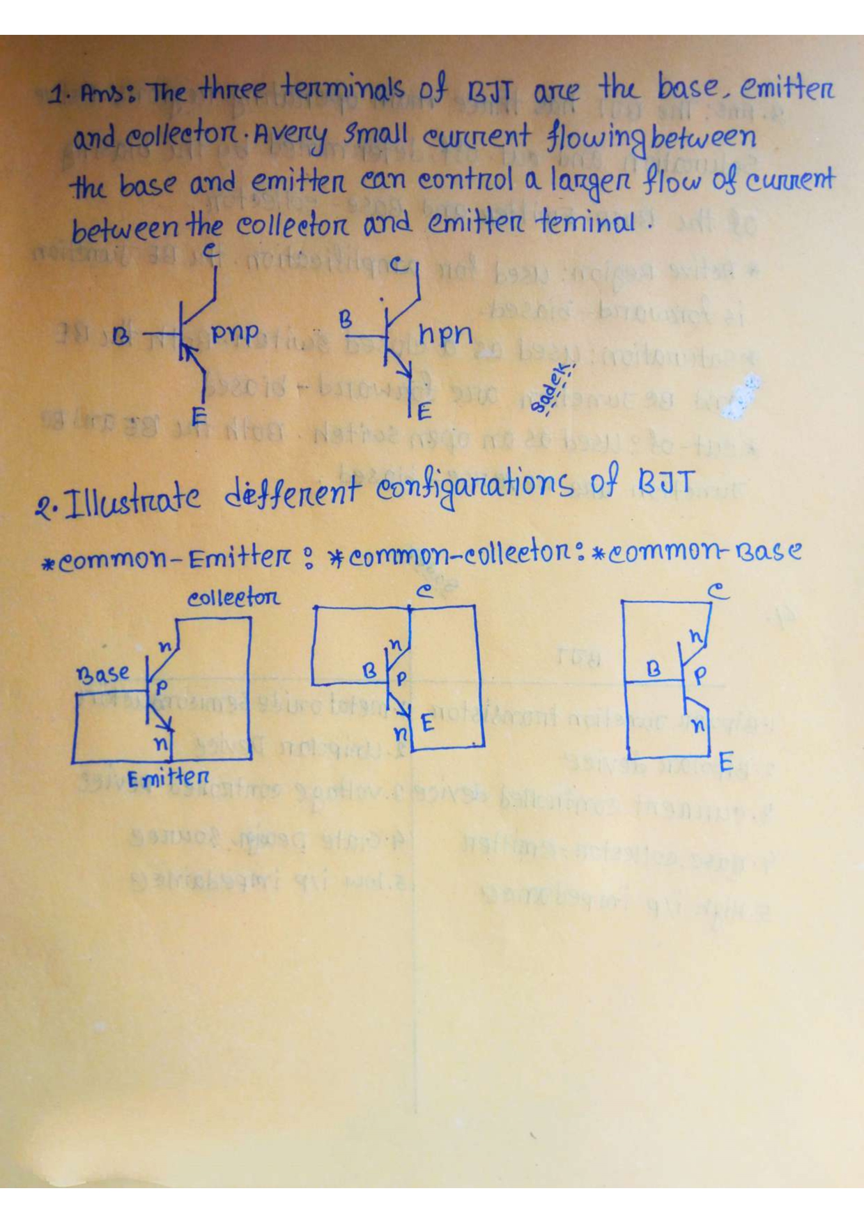
Definition: A BJT is a three-terminal semiconductor device consisting of two PN junctions. It has three regions: Emitter (E), Base (B), and Collector (C). Current flow involves both electrons and holes (bipolar).
Q6. BJT Configurations.4 Marks
Three basic configurations based on which terminal is common:
| Configuration | Input | Output | Current Gain | Voltage Gain | Applications |
|---|---|---|---|---|---|
| Common Emitter (CE) | Base-Emitter | Collector-Emitter | High (β) | High | Amplifiers, Switching |
| Common Base (CB) | Emitter-Base | Collector-Base | Low (<1) | High | High-frequency amplifiers |
| Common Collector (CC) | Base-Collector | Emitter-Collector | High | Low (<1) | Impedance matching, Buffers |
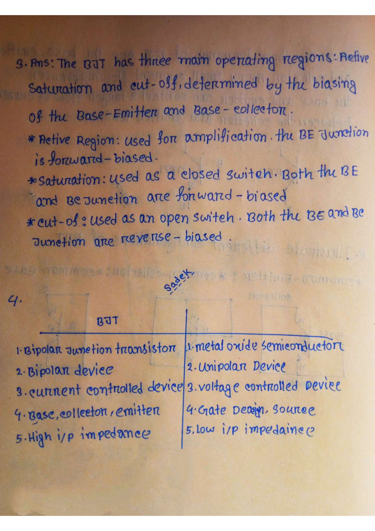
Q7. BJT Operating Modes (Junction Biases).4 Marks
BJT has two junctions: Emitter-Base (EB) and Collector-Base (CB). Four operating modes:
| Operating Mode | EB Junction | CB Junction | Application |
|---|---|---|---|
| Active/Linear | Forward Biased | Reverse Biased | Amplification |
| Saturation | Forward Biased | Forward Biased | ON switch (Digital) |
| Cutoff | Reverse Biased | Reverse Biased | OFF switch (Digital) |
| Inverse Active | Reverse Biased | Forward Biased | Rarely used |
Q8. Types of Transistors.2 Marks
- BJT (Bipolar Junction Transistor):
- NPN Transistor
- PNP Transistor
- FET (Field Effect Transistor):
- JFET (Junction FET) - N-channel, P-channel
- MOSFET (Metal Oxide Semiconductor FET)
- Enhancement Mode (E-MOSFET)
- Depletion Mode (D-MOSFET)
Q9. Characteristics of BJT.3 Marks
Key Characteristics:
- Current-controlled device: IC depends on IB
- Low input impedance: Few hundred ohms
- High output impedance: Several kΩ
- Temperature sensitive: Performance varies with temperature
- Power consumption: Higher than FET
- Switching speed: Moderate (slower than MOSFET)
- Gain (β): Typically 50-200
Three Main Characteristics:
- Input Characteristics: IB vs VBE (VCE constant)
- Output Characteristics: IC vs VCE (IB constant)
- Transfer Characteristics: IC vs IB (VCE constant)
Q10. Applications of Transistors.2 Marks
- Amplification: Audio, RF, and power amplifiers
- Switching: Digital circuits, logic gates
- Oscillators: Signal generation
- Voltage Regulation: Power supplies
- Signal Processing: Modulation, demodulation
- Motor Control: Speed and direction control
Section C: MOSFET
Q11. Define MOSFET with Symbol.3 Marks
Definition: MOSFET (Metal Oxide Semiconductor Field Effect Transistor) is a voltage-controlled three-terminal device with Gate (G), Drain (D), and Source (S). Current flow is controlled by electric field.

Q12. BJT vs MOSFET Comparison.5 Marks
| Parameter | BJT | MOSFET |
|---|---|---|
| Control Type | Current-controlled (IB controls IC) | Voltage-controlled (VGS controls ID) |
| Terminals | Emitter, Base, Collector | Source, Gate, Drain |
| Input Impedance | Low (few hundred Ω) | Very High (MΩ range) |
| Current Flow | Bipolar (electrons & holes) | Unipolar (electrons or holes) |
| Switching Speed | Moderate | Fast |
| Power Consumption | Higher | Lower |
| Temperature Stability | Less stable | More stable |
| Noise | Higher | Lower |
| Size | Larger | Smaller (IC applications) |
| Cost | Lower | Higher |
| Applications | Audio amplifiers, linear circuits | Digital circuits, switching, VLSI |
Section D: Problem Solving
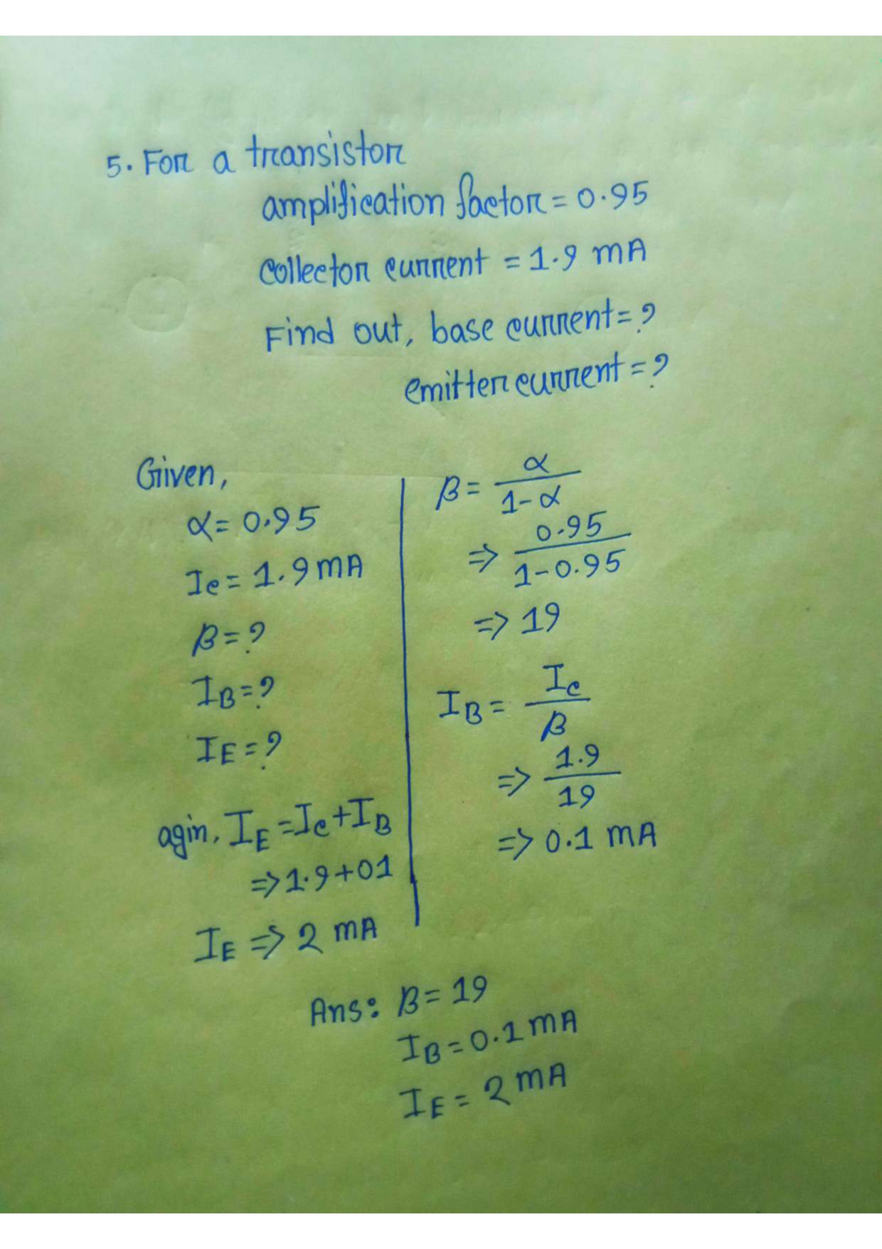
Q13. Given: α = 0.95, IC = 1.9 mA. Find β, IE, and IB.5 Marks
Given:
- Amplification factor (α) = 0.95
- Collector current (IC) = 1.9 mA
Formulas:
Solution:
Step 1: Find Current Gain (β)
Step 2: Find Base Current (IB)
Step 3: Find Emitter Current (IE)
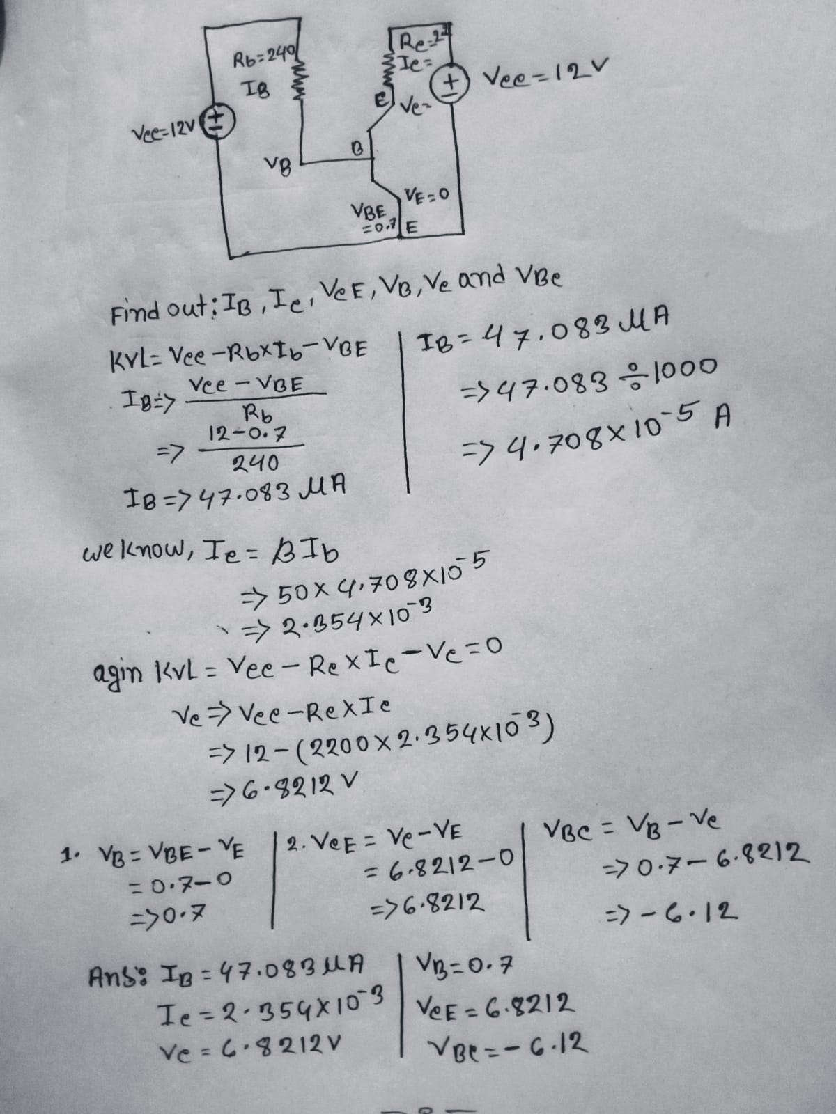
Q14. Given: β = 50, VCC = 12V, RB = 240 kΩ, RC = 2.2 kΩ (Silicon). Find IB, IC, VCE, VB, VC, VBC. 8 Marks
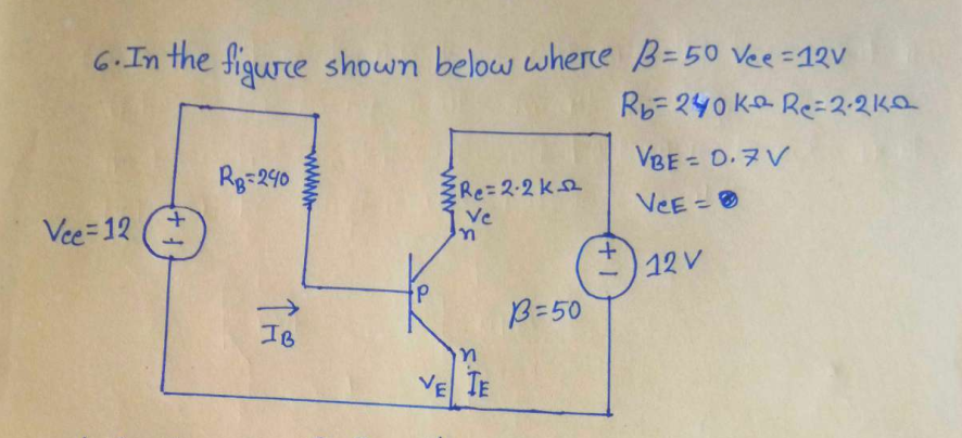
Given: β = 50, VCC = 12V, RB = 240 kΩ, RC = 2.2 kΩ
Assume: Silicon transistor ⇒ VBE = 0.7V, VE = 0
Step 1: Base Current (IB)
Step 2: Collector Current (IC)
Step 3: Collector Voltage (VC)
Step 4: Collector-Emitter Voltage (VCE)
Step 5: Base Voltage (VB)
Step 6: Base-Collector Voltage (VBC)
IB = 47 µA, IC = 2.35 mA, VC = 6.83 V,
VCE = 6.83 V, VB = 0.7 V, VBC = −6.13 V
(VBC negative ⇒ transistor operates in active region)
Q15. Additional Important Formulas.2 Marks
Current Relations:
Typical Values:
- α: 0.95 to 0.99
- β: 20 to 200
- VBE (Silicon): 0.7V
- VBE (Germanium): 0.3V
Section E: Additional Topics
Q16. Transistor as an Amplifier.3 Marks
In active region, small changes in base current cause large changes in collector current.
- Voltage Gain (AV): AV = Vout / Vin = -β × (RC / Rin)
- Current Gain (AI): AI = IC / IB = β
- Power Gain (AP): AP = AV × AI
CE configuration provides both voltage and current gain, making it most popular for amplification.
Q17. Transistor as a Switch.3 Marks
Transistor operates between cutoff (OFF) and saturation (ON):
- Cutoff Mode (OFF): IB = 0, IC ≈ 0, VCE ≈ VCC (Open switch)
- Saturation Mode (ON): IB is large, IC = VCC/RC, VCE ≈ 0.2V (Closed switch)
Applications: Digital logic gates, relay drivers, LED drivers, motor control
Q18. Biasing Techniques.2 Marks
- Fixed Bias: Simple but temperature unstable
- Voltage Divider Bias: Most stable, widely used
- Emitter Bias: Good stability with negative supply
- Collector Feedback Bias: Moderate stability
Q20. Advantages and Disadvantages.3 Marks
BJT Advantages:
- High current handling capacity
- Better for analog/linear applications
- Lower cost
- Higher transconductance
BJT Disadvantages:
- Lower input impedance
- Temperature sensitive
- Slower switching speed
- Requires continuous base current
Most important Questions from teacher in the class
Exam Preparation Complete!
Total Questions: 20 | Total Marks: 60
Study Focus: Diode characteristics, BJT configurations, Operating modes, Problem solving
Good Luck for Your Final Exam!